
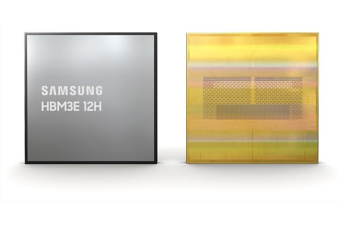
Samsung announced late on Monday the completion of the development of its 12-Hi 36 GB HBM3E memory stacks, just hours after Micron said it had kicked off mass production of its 8-Hi 24 GB HBM3E memory products. The new memory packages, codenamed Shinebolt, increase peak bandwidth and capacity compared to their predecessors, codenamed Icebolt, by over 50% and are currently the world’s fastest memory devices.
As the description suggests, Samsung’s Shinebolt 12-Hi 36 GB HBM3E stacks pack 12 24Gb memory devices on top of a logic die featuring a 1024-bit interface. The new 36 GB HBM3E memory modules feature a data transfer rate of 10 GT/s and thus offer a peak bandwidth of 1.28 TB/s per stack, the industry’s highest per-device (or rather per-module) memory bandwidth.
Meanwhile, keep in mind that developers of HBM-supporting processors tend to be cautious, so they will use Samsung’s HBM3E at much lower data transfer rates to some degree because of power consumption and to some degree to ensure ultimate stability for artificial intelligence (AI) and high-performance computing (HPC) applications.
Samsung HBM Memory Generations
HBM3E
(Shinebolt)
HBM3
(Icebolt)
HBM2E
(Flashbolt)
HBM2
(Aquabolt)
Max Capacity
36GB
24 GB
16 GB
8 GB
Max Bandwidth Per Pin
9.8 Gb/s
6.4 Gb/s
3.6 Gb/s
2.0 Gb/s
Number of DRAM ICs per Stack
12
12
8
8
Effective Bus Width
1024-bit
Voltage
?
1.1 V
1.2 V
1.2 V
Bandwidth per Stack
1.225 TB/s
819.2 GB/s
460.8 GB/s
256 GB/s
To make its Shinebolt 12-Hi 36 GB HBM3E memory stacks, Samsung had to use several advanced technologies. First, the 36 GB HBM3E memory products are based on memory devices made on Samsung’s 4th generation 10nm-class (14nm) fabrication technology, which is called and uses extreme ultraviolet (EUV) lithography.
Secondly, to ensure that 12-Hi HBM3E stacks have the same z-height as 8-Hi HBM3 products, Samsung used its advanced thermal compression non-conductive film (TC NCF), which allowed it to achieve the industry’s smallest gap between memory devices at seven micrometers (7 µm). By shrinking gaps between DRAMs, Samsung increases vertical density and mitigates chip die warping. Furthermore, Samsung uses bumps of various sizes between the DRAM ICs; smaller bumps are used in areas for signaling. In contrast, larger ones are placed in spots that require heat dissipation, which improves thermal management.
Samsung estimates that its 12-Hi HBM3E 36 GB modules can increase the average speed for AI training by 34% and expand the number of simultaneous users of inference services by more than 11.5 times. However, the company has not elaborated on the size of the LLM.
Samsung has already begun providing samples of the HBM3E 12H to customers, with mass production scheduled to commence in the first half of this year.
Source: Samsung


